Crystallographic defects are deviations from an ideal microscopic lattice structure of metals such as vacancies or dislocations.
Introduction
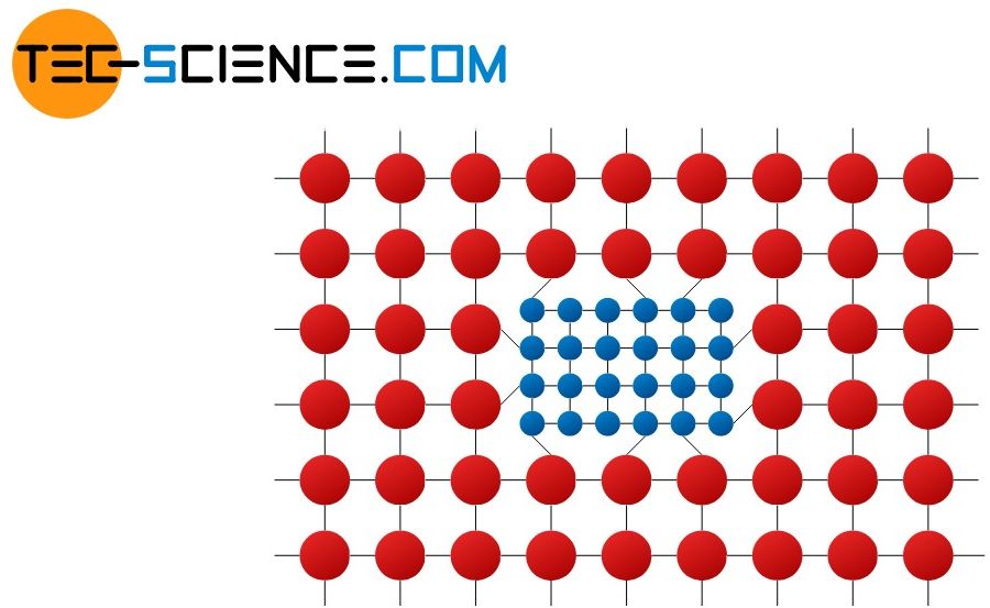
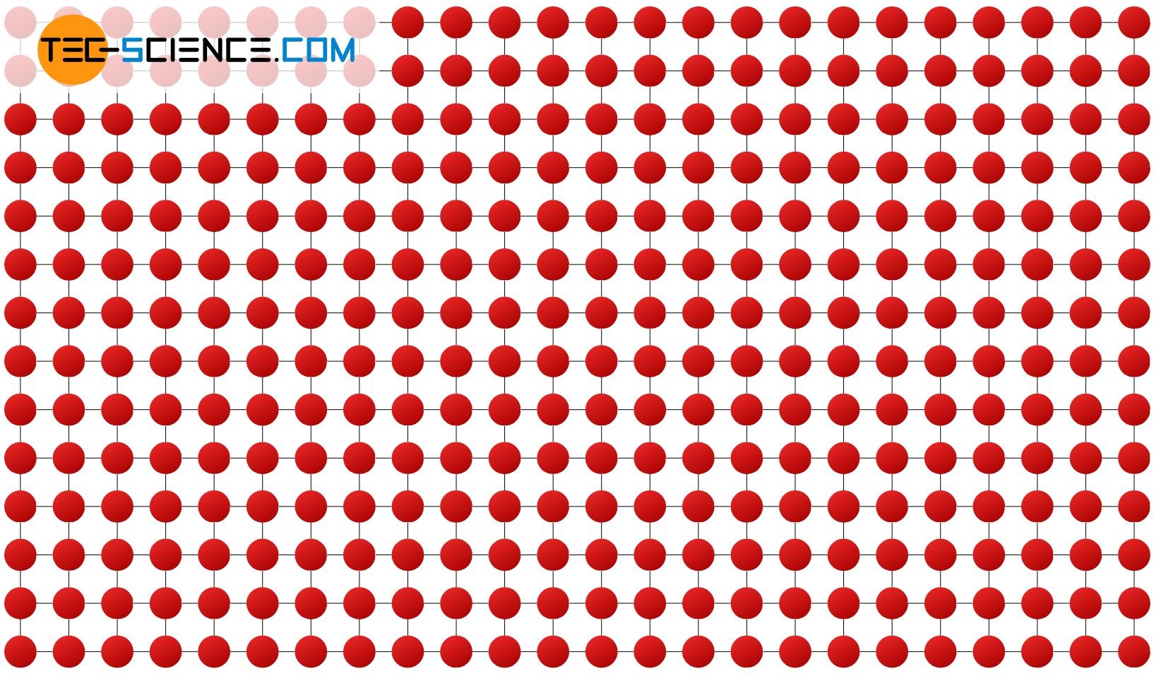
The previous article dealt with a uniform and error-free structure of the metals. However, such ideal crystals do not exist in reality or can only be achieved approximately on a very small scale under extreme expense (for example in so-called whiskers).
Real metals do not have a perfect lattice structure but show so-called crystallographic defects. At these defects, the real lattice deviates from the idealized perfect structure.
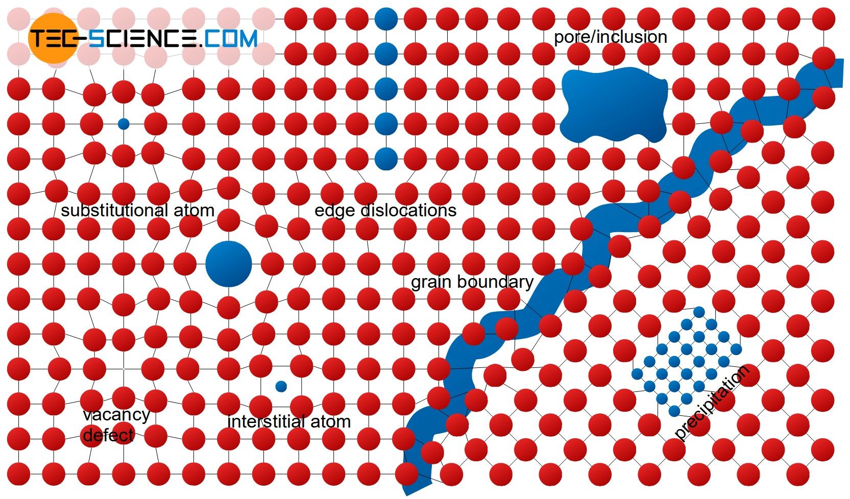
The figure above shows examples of different crystallographic defects, which can be subdivided depending on their impact on the surrounding structure. The following sections discuss these types of impurities more closely:
- 0-dimensional crystallographic defects (punctiform defects)
- 1-dimensional crystallographic defects (linear defects)
- 2-dimensional crystallographic defects (area-shaped defects)
- 3-dimensional crystallographic defects (volume-shaped defects)
Point defects
Point defects are also referred to as 0-dimensional defects and disturb the lattice only within a very limited (punctiform) region. The following sections discuss these types of point defects:
- vacancies
- Substitutional atoms
- Interstitial atoms
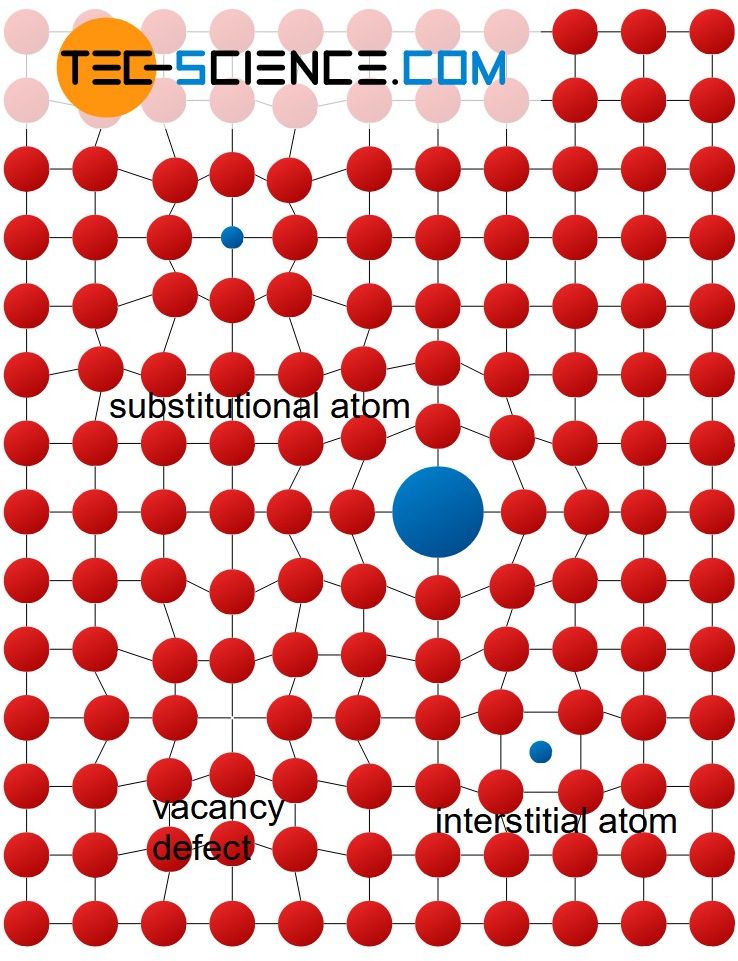
Vacancies
The vacancies are sites in the structure that are not occupied by an atom and thus remain vacant. The vacancy density usually increases exponentially with increasing temperature. The reason for this is the increased lattice vibration, which “tears” some atoms from their regular sites. If the atoms migrate by self-diffusion to the metal surface, they leave a vacancy defect in the material. However, this also means that vacancies in a metal can not be avoided in principle, since they are in a thermodynamic equilibrium. These types of vacancies are also called thermal vacancies.
Vacancies are unoccupied sites in the lattice structure. They are usually in thermodynamic equilibrium and can not be avoided!
At 1 quadrillion (1015) atoms comes at room temperature about one vacancy. Immediately below the melting temperature already one vacancy comes at 10,000 atoms (104).
Vacancies can also be “trapped” in the material by rapid cooling from the hot state. However, these are not in thermodynamic equilibrium and partially heal over time due to diffusion processes (athermal vacancies).
Substitutional atom
However, there are not only vacancies interfering with a lattice structure. In addition, a metal is not free of foreign atoms. In the lattice structure, these foreign atoms can displace the actual metal atoms and thus occupy their lattice sites. Since the actual metal atom has been substituted by the foreign atom, it is also called a substitutional atom.
Substitutional atoms are foreign atoms which are occupying regular sites!
Interstitial atoms
A further possibility of the arrangement of foreign atoms consists in the storage on an interstitial space, e.g. in the cube center of a face-centered cubic unit cell (also referred to as octahedral site). Atoms that are not on regular sites but have interposed therebetween, are referred to as interstitial atoms.
Interstitial atoms do not occupy regular sites but interstitial sites.
Foreign atoms can migrate (diffuse) particularly well through the material due to lattice vibrations if there are many vacancies. There is plenty of room to get from one vacancy to another. Therefore, vacancies play an important role in diffusion processes of foreign atoms!
Line defects
Line defects are also called 1-dimensional crystallographic defects. They disturb the crystalline structure within a larger area compared to point defects. This only includes the so-called edge dislocations and the screw dislocations:
- edge dislocations
- screw dislocations
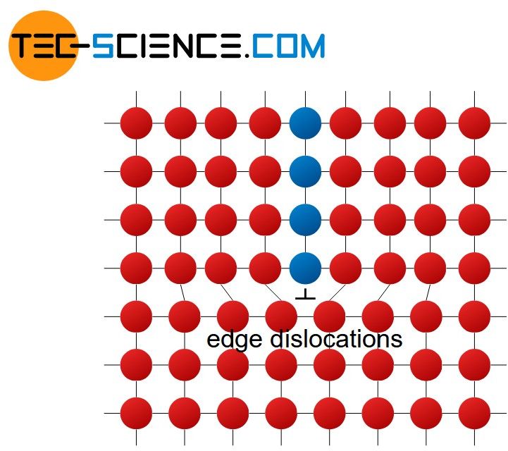
A edge dislocation is a lattice plane that ends in the metal structure without further connection. It can be thought of as an inserted atomic plane in the already existing structure. The “edge” of this inserted atomic plane is also referred to as a dislocation line or dislocation core and often symbolized in drawings with a “T”. Along these dislocation lines, the lattice structure is heavily distorted and has stresses. The dislocation line either forms a closed ring or exits the surface of the crystal (grain) or terminates at other defects.
A edge dislocation is an inserted atomic plane that is not continued in the lattice structure!
In contrast to a edge dislocation, a screw dislocation winds an atomic plane along the dislocation line through the crystal like the thread of a screw. In a crystal always combinations of both types of dislocation occur.
Dislocations occur during solidification of melts or due to stresses in the metal. But they are also introduced by plastic deformation (work hardening or strain hardening). Dislocations play a central role in deformation processes, since they are largely responsible for the good ductility of the metals.
Dislocations play a central role in the ductility of metals!
The dislocation density in a crystal is given as the total length of all dislocation lines per volume. Dislocation lines with a total length of about 1 km are found per square millimeter in a metal. Cold working increases the dislocation length per square millimeter to around 1 million kilometers! From a dislocation density of about 100 million kilometers per square millimeter, however, the material is so damaged that it is destroyed in principle.
Planar defects
Compared to linear crystallographic defects, planar defects disturb the lattice structure in a spatially larger area. The following defects fall into this categorization of the so-called 2-dimensional defects:
- high angle grain boundaries
- low angle grain boundaries
- phase boundaries
- stacking fault
Grain boundary
Grain boundaries delimit areas in a crystal within the lattice structure shows a uniform spatial orientation. These boundaries are structureless regions of thickness on the order of only 2 to 4 atomic distances. The uniformly aligned areas themselves are referred to as grains or as crystallites. The unit cells are identical for each grain, they only have a different spatial orientation (rotated, mirrored, etc.).
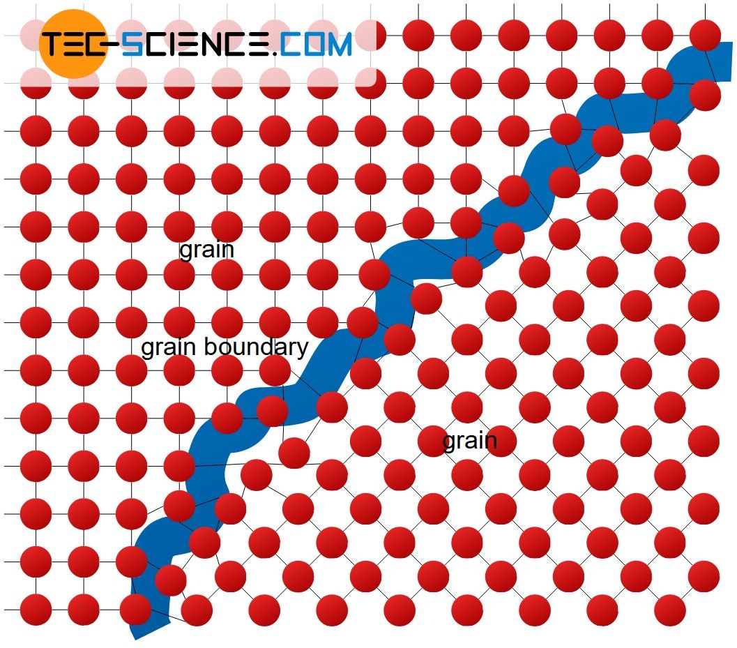
The grain structure is formed during the solidification of the molten metal, since a melt usually does not solidify starting from a single point but at many points at the same time (exception: single crystals or monocrystals!). At each of these solidification points (so-called nuclei), the lattice structure is formed with its own orientation. The growing grains collide after complete solidification of the melt and thus form the grain boundaries.
Grain refers to a crystal region with a uniform spatial lattice orientation. Different grains are separated by grain boundaries!
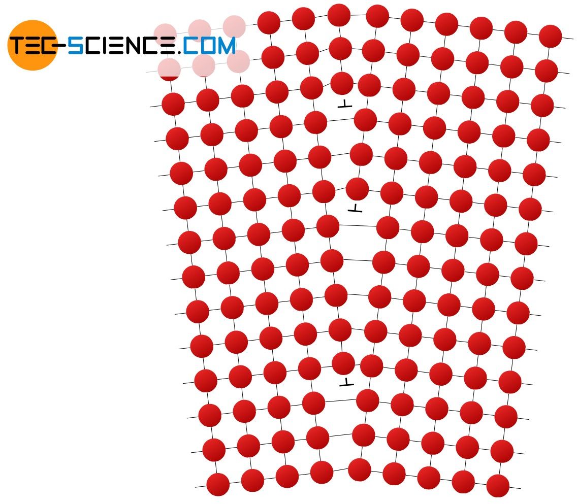
Small angle grain boundary
A deviation of the crystal orientation can also arise if several dislocations are superimposed. Since these errors change the lattice orientation by only a few degrees (<15 °), one also speaks of a low angle grain boundary. Due to the better delimitation, the grain boundaries described above are often referred to as high angle grain boundaries.
Twin grain boundary
A special type of grain boundary is the so-called twin boundary. In this case, the opposing lattice structures are just ordered in mirror image. Such a twin grain boundary has a high symmetry and thus low energy.
Twin boundaries are often seen under the microscope as straight lines, while “normal” grain boundaries are characterized by more curvy lines. Twin grain boundaries are very often formed in metals like brass, copper and austenite (γ-Fe).
While grain boundaries generally form incoherent interfaces, twin grain boundaries show a fully coherent interface (for the concept of coherence, see the next section).
Phase boundary
The so-called phase boundary forms another type of planar crystallographic defects.
A phase is a space with a uniform chemical structure!
A phase may be an accumulation of alloying elements in the host lattice of the metal. Thus a phase boundary spatially delimits two different chemical structures. Depending on how the structures of the different phases merge, a distinction is made between a coherent, partially coherent or incoherent phase boundary.
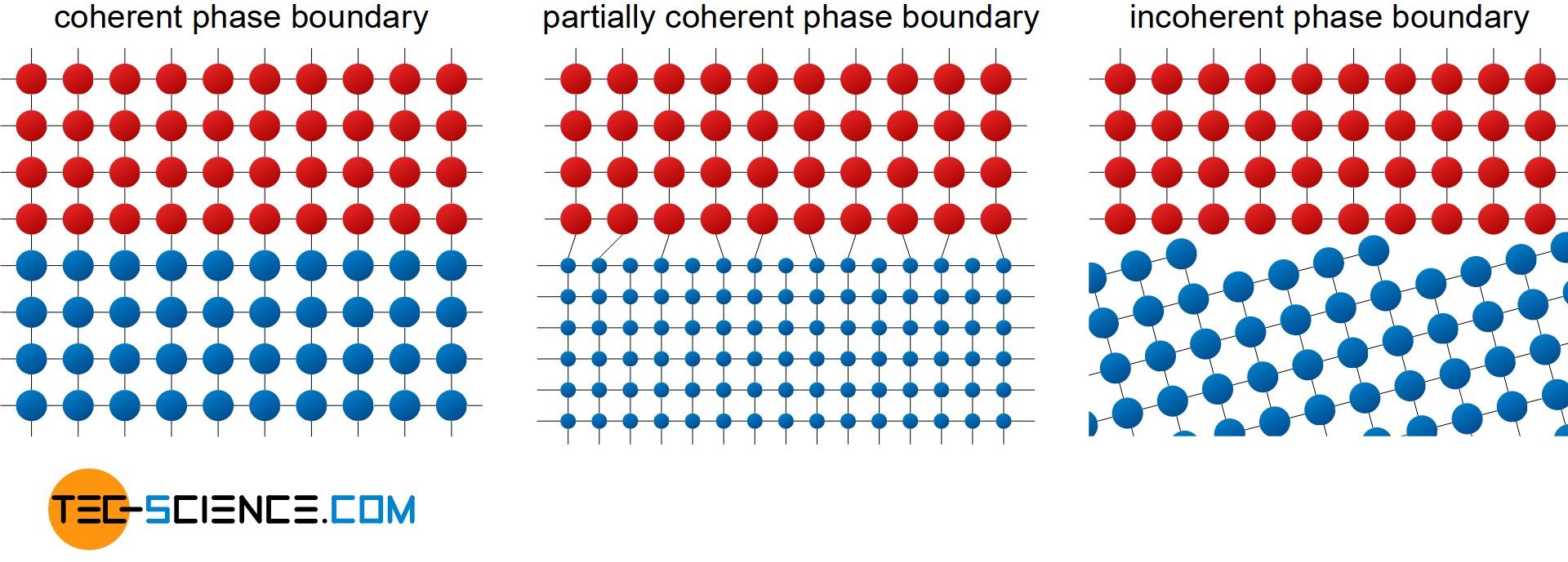
With a coherent phase boundary, the two structures merge into one another without any gaps. This is true if the two phases have a consistent structure and similar chemical properties.
However, if the phases differ somewhat in their properties, the lattice structures no longer completely merge into one another. Therefore dislocations must be present at regular intervals. One then speaks of a partially coherent phase boundary..
By contrast, with an incoherent phase boundary, neither the lattice structures nor the chemical properties of the two phases match. The structure is similar to a high angle grain boundary, but consists of two distinct phases. The phase boundaries are not distorted to the extent that is the case with high angle grain boundaries.
Stacking fault
Another planar defect is the so-called stacking fault. It is a locally different stacking sequence of otherwise periodically arranged planes. For example, the stacking sequence of the closest packed planes in the face-centered cubic lattice with normally ABCABC may locally have the sequence ABACAB. Such stacking faults can arise when a dislocation is split into two smaller dislocations.
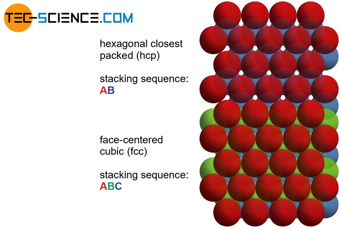
Stacking faults are local deviations from the actual stacking sequence of the lattice structure!
Bulk defects
Bulk defects are also referred to as 3-dimensional defects and interfere with the lattice structure to a greater extent than the planar defects do:
- precipitations
- pores
- inclusions
The so-called precipitations are an accumulation of chemical compounds (phases) in the metal. In addition to precipitations, pores or other inclusions are among the 3-dimensional defects.