The solidification of a melt starts from nuclei, resulting in the typical polycrystal microstructure.
Polycrystal
A metallic material generally does not have a uniform lattice orientation (see crystallographic defects). Exceptions to this are single crystals, which, however, can only be produced at great technical expense (more on this later).
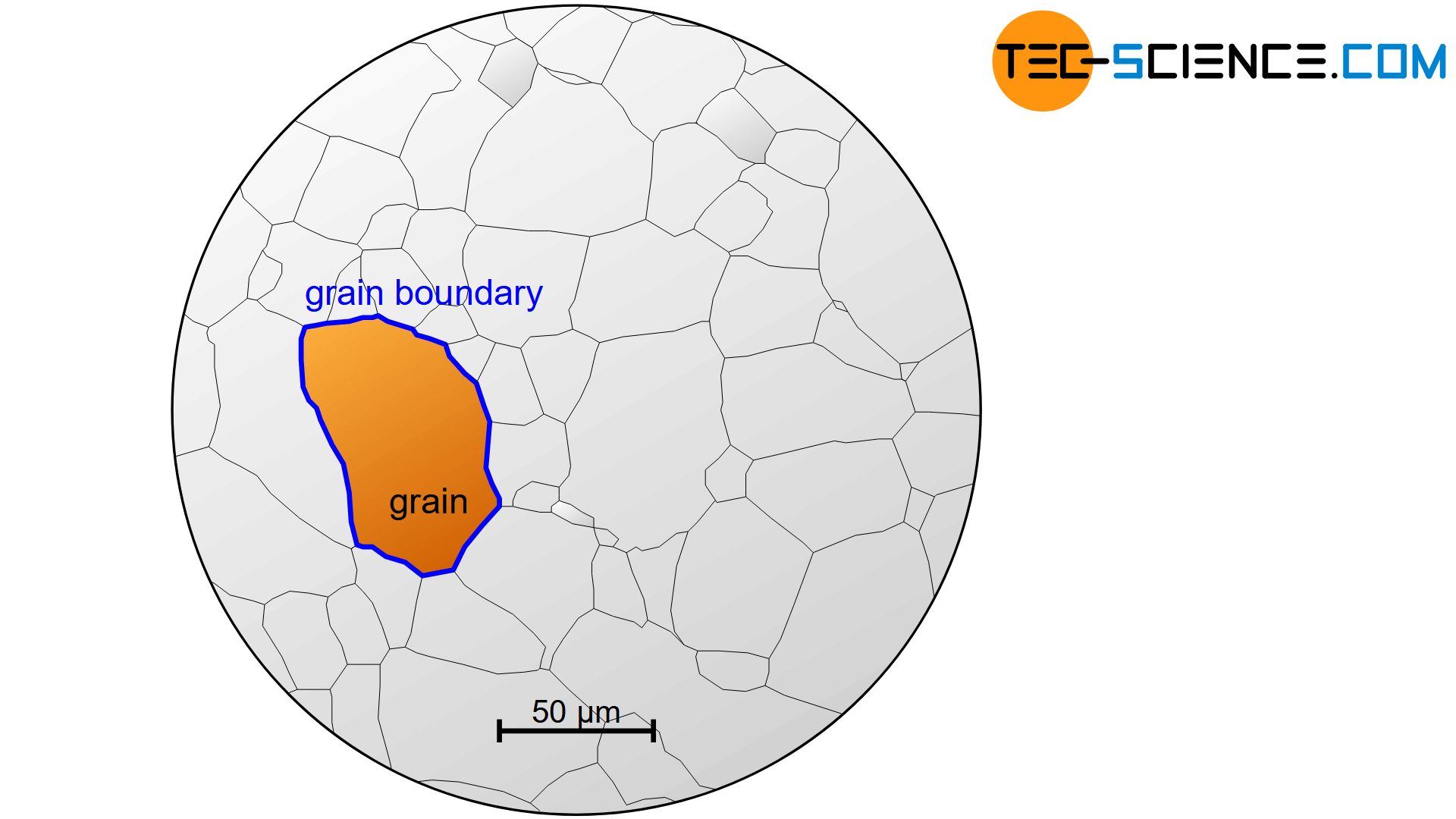
In general, metals have microscopic areas, in which the orientation of the lattice structure change from area to area (the term lattice orientation must not be confused with the term lattice structure!). These small zones of constant lattice orientation are called grains or crystallites. The different grains are separated by relatively structureless regions, which are only a few atomic distances wide. These regions are called grain boundaries.
Grains (crystallites) are small areas within a crystalline material which have a uniform lattice orientation. Individual grains are separated by grain boundaries!
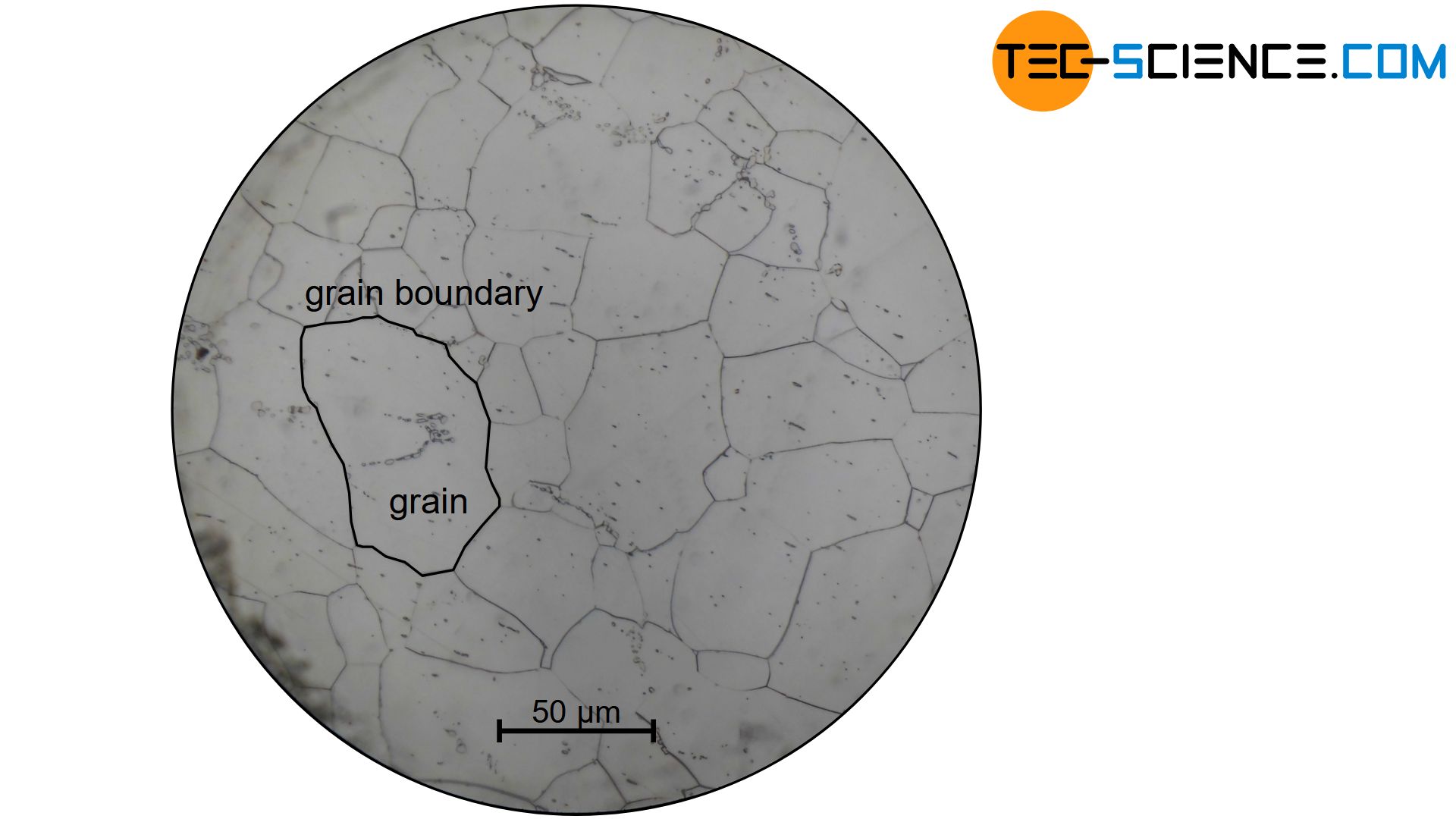
The light micrograph above shows iron in an almost carbon-free state. One can see the individual grains (white areas) with their grain boundaries and silicate inclusions (dark spots).
One calls such a microscopically visible structure in the interior of a material with its grains, grain boundaries, precipitates, etc. also microstructure.
Microstructures are the microscopic structure of a substance!
In a micrograph, microstructures can be seen. For this, however, the sample must be specially prepared in most cases. In particular by polishing and etching (for example with alcoholic nitric acid). Since the different lattice orientation of the grains is accompanied by a different reflection behavior, they are clearly distinguishable under a microscope. Such a crystal, which is characterized by many small crystallites (grains), is also called polycrystal.
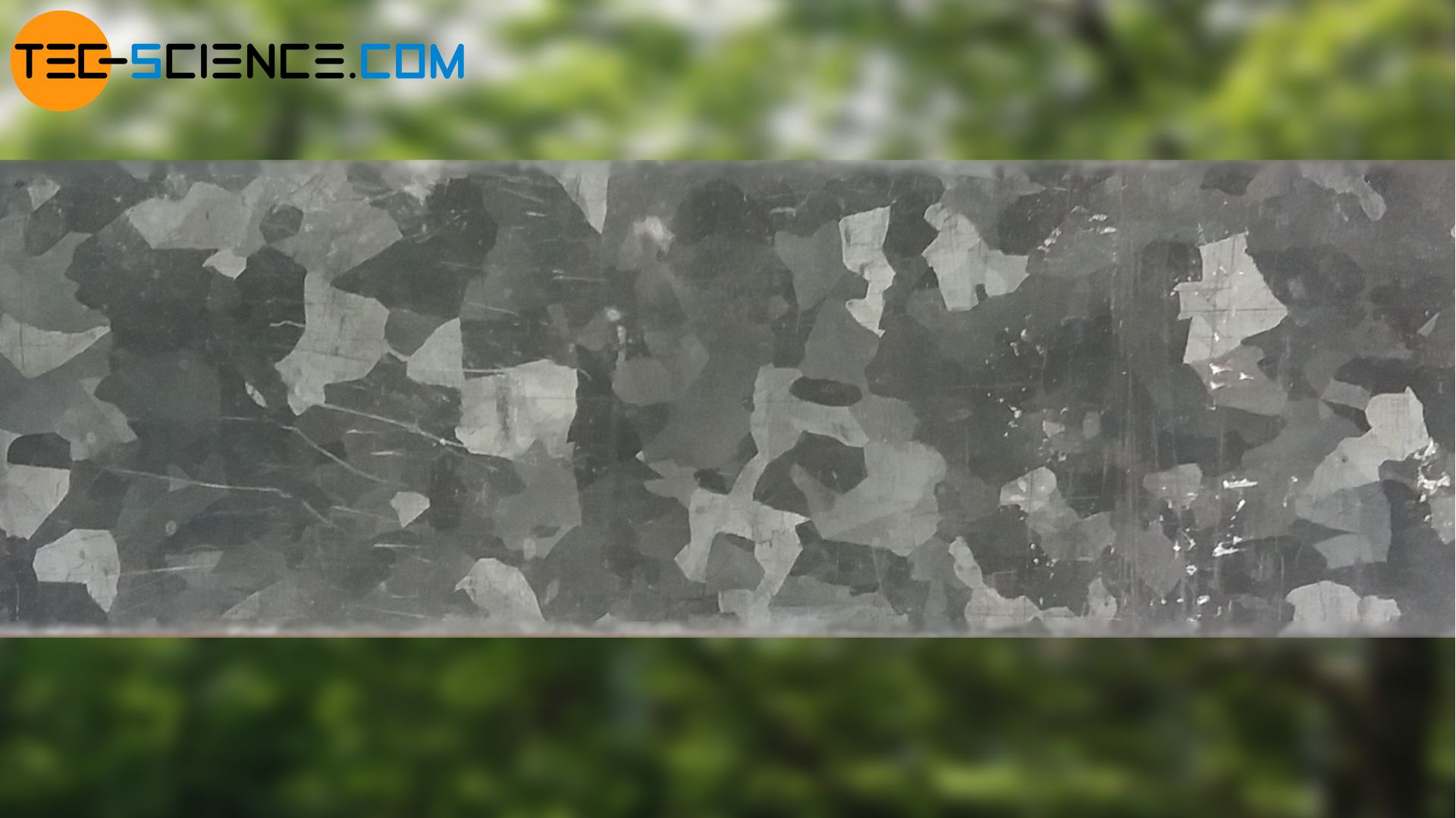
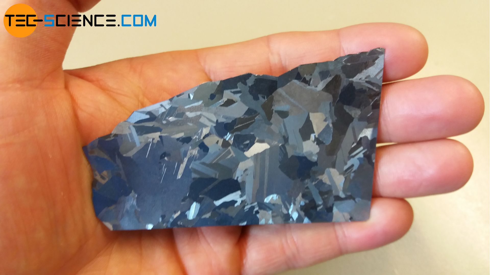
In cases such as polycrystalline silicon solar cells or galvanized sheet, the individual grains are visible even to the naked eye. The picture below shows a galvanized component made of steel and a polycrystalline silicon solar cell.
It is often useful to draw a micrograph only schematically to make the essential structure of the material visible. The figure below shows the schematic microstructure of a polycrystalline material.
Solidification process
A grainy microstructure as seen in the upper section is typical for metals. The reason for this lies in the solidification process. Liquid metals usually do not start to solidify in a single point. Rather, the solidification process starts at many points of the melt simultaneously. Such solidification points are generally referred to as nuclei. The formation of the crystal structure is also called crystallization.
The solidification process in crystalline materials is also referred to as crystallization!
Each nucleus initiated the formation of the lattice structure. The spatial orientation of the lattice is different from nucleus to nucleus, depending on how the nucleus is aligned in the melt. Each nucleus will later become a grain with a uniform lattice orientation. Where the grains collide after crystallization, the grain boundaries arise.
Grain boundaries are among the two-dimensional crystallographic defects, since they interfere with the uniform lattice orientation. However, this does not have to be a disadvantage, as one could prematurely draw from the term “defect”. Grain boundaries even contribute in particular to increase the strength (grain boundary hardening), since the deformation mechanism is blocked at the grain boundaries. Fine-grained metals with many grain boundaries are thus characterized by a relatively high strength combined with good toughness.
Fine-grained microstructures usually have good toughness and high strength at the same time!
This raises the question of how one can influence the structure of a metal so that many grains are formed in the structure. To clarify this question, the process of solidification needs to be considered more closely. Therefore, in a separate article, the conditions of solidification are dealt with in more detail.
Monocrystal (single crystal)
In contrast to a polycrystal, however, a monocrystal consists of only one single grain. At the atomic level, such a single crystal is characterized by a uniform lattice orientation. This means in particular that the microstructure has no grain boundaries.
A single crystal consists of only one single grain with a certain spatial lattice orientation!
Single crystals can be specially grown out of the melt by certain methods. The solidification process is not initiated simultaneously as usual in many places at the same time but only triggered at a single point (on a so-called seed crystal). The melt then solidifies with a uniform lattice orientation.

Such a principle is used, for example, as a so-called Czochralski process in chip manufacture. There, single crystals are needed so that the electrical conductivity is not adversely affected by grain boundaries or other lattice orientations.
But also as a construction material single crystals are used in special cases. For example, as high-strength turbine blades (nickel superalloy) in high-temperature range. Especially in high-temperature applications, a polycrystalline material has the disadvantage that the grain boundaries start to shift above the recrystallization temperature (called grain boundary sliding). The material “softens”, so to speak. Consequently, to prevent this “softening”, a high temperature material must not have grain boundaries, especially at high load.


